
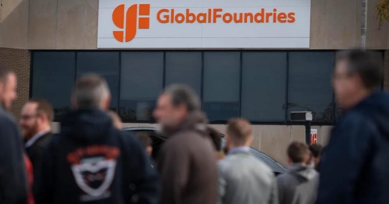
GlobalFoundries hits production readiness on SLATE bonding tech, signaling semiconductor supply chain shifts that matter for crypto mining

GlobalFoundries hits production readiness on SLATE bonding tech, signaling semiconductor supply chain shifts that matter for crypto mining

The chipmaker's new wafer-to-wafer bonding technology promises 45% smaller dies, with downstream implications for the hardware powering everything from 5G to data centers.

GlobalFoundries just cleared a major engineering milestone. The specialty semiconductor manufacturer announced production readiness for its SLATE wafer-to-wafer bonding technology, a process that enables vertical stacking of transistors and shrinks die sizes by up to 45%.

Volume production is slated to begin in the second half of 2027 at the company’s 300mm fabrication facility in Singapore.

What SLATE actually does

The technology enables homogeneous wafer-to-wafer bonding on GlobalFoundries’ 9SW radio-frequency silicon-on-insulator platform, which launched in 2023. Instead of laying transistors flat across a chip, you stack them like floors in a building.

Advertisement

The result is a die size reduction of up to 45%. This matters for cellular front-end modules, the components that handle signal processing in your phone, including switches, low-noise amplifiers, and antenna tuners.

GlobalFoundries has already outlined a roadmap extending SLATE’s heterogeneous 3D integration capabilities to its FDX FD-SOI and silicon germanium technologies. Target markets span mobile, IoT, data centers, and satellite connectivity.

Design migration for SLATE is supported through PDK-driven flows, meaning existing chip designs can be adapted to the new 3D process without starting from scratch.

What investors should watch

GlobalFoundries trades on Nasdaq under GFS. The company focuses on mature and specialty nodes rather than competing at sub-3nm process nodes the way TSMC does, serving markets including automotive, industrial, communications, and defense.

Successful deployment would expand GlobalFoundries’ addressable market in RF front-end modules, a segment expected to grow as 5G networks continue their global rollout.

The Singapore manufacturing location carries strategic significance as US-China tensions continue to reshape global chip supply chains, positioning facilities outside of Taiwan and mainland China with a geographic premium.

Disclosure: This article was edited by Editorial Team. For more information on how we create and review content, see our Editorial Policy.

GlobalFoundries hits production readiness on SLATE bonding tech, signaling semiconductor supply chain shifts that matter for crypto mining

GlobalFoundries hits production readiness on SLATE bonding tech, signaling semiconductor supply chain shifts that matter for crypto mining

The chipmaker's new wafer-to-wafer bonding technology promises 45% smaller dies, with downstream implications for the hardware powering everything from 5G to data centers.

GlobalFoundries just cleared a major engineering milestone. The specialty semiconductor manufacturer announced production readiness for its SLATE wafer-to-wafer bonding technology, a process that enables vertical stacking of transistors and shrinks die sizes by up to 45%.

Volume production is slated to begin in the second half of 2027 at the company’s 300mm fabrication facility in Singapore.

What SLATE actually does

The technology enables homogeneous wafer-to-wafer bonding on GlobalFoundries’ 9SW radio-frequency silicon-on-insulator platform, which launched in 2023. Instead of laying transistors flat across a chip, you stack them like floors in a building.

Advertisement

The result is a die size reduction of up to 45%. This matters for cellular front-end modules, the components that handle signal processing in your phone, including switches, low-noise amplifiers, and antenna tuners.

GlobalFoundries has already outlined a roadmap extending SLATE’s heterogeneous 3D integration capabilities to its FDX FD-SOI and silicon germanium technologies. Target markets span mobile, IoT, data centers, and satellite connectivity.

Design migration for SLATE is supported through PDK-driven flows, meaning existing chip designs can be adapted to the new 3D process without starting from scratch.

What investors should watch

GlobalFoundries trades on Nasdaq under GFS. The company focuses on mature and specialty nodes rather than competing at sub-3nm process nodes the way TSMC does, serving markets including automotive, industrial, communications, and defense.

Successful deployment would expand GlobalFoundries’ addressable market in RF front-end modules, a segment expected to grow as 5G networks continue their global rollout.

The Singapore manufacturing location carries strategic significance as US-China tensions continue to reshape global chip supply chains, positioning facilities outside of Taiwan and mainland China with a geographic premium.

Disclosure: This article was edited by Editorial Team. For more information on how we create and review content, see our Editorial Policy.