Huawei develops 122TB SSD using innovative packaging amid US export controls
Cut off from the world's most advanced memory chips, Huawei engineered around the problem with a packaging trick that boosts storage density by 33%.
When you can’t get the best chips, you figure out how to fit more of the chips you can get. That’s essentially what Huawei just did.
The Chinese tech giant unveiled enterprise SSDs with capacities of 61.44 TB and 122.88 TB at the Huawei ID Forum 2026 in Paris, held May 21-23. The secret sauce is a proprietary technique called Die-on-Board (DoB) packaging, which mounts NAND flash dies directly onto the printed circuit board rather than using conventional packaging methods. The result: roughly 33% higher density from the same underlying memory technology.
The packaging play
US sanctions have forced Huawei to rely on domestic NAND suppliers, primarily YMTC (Yangtze Memory Technologies Co.), whose chips top out at approximately 232 layers. So Huawei’s engineering team couldn’t win on the vertical stacking front. Instead, DoB packaging eliminates traditional chip packaging overhead, letting engineers mount more dies directly onto the PCB and squeeze additional capacity from each drive.
Huawei isn’t stopping at 122 TB. A 245 TB variant is already reportedly in production.
Real-world deployment numbers
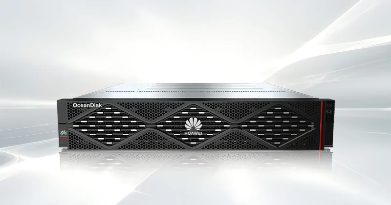
Huawei is already integrating the 122.88 TB drives into its OceanStor Pacific 9926 all-flash array. Pack 36 of those drives into a single system, and you get 4.42 PB of raw storage. With data compression applied, effective capacity stretches to approximately 11 PB.
The drives are purpose-built for AI inference, data center operations, and scale-out storage.
Why this matters beyond storage
US export controls were designed, in part, to slow China’s AI and advanced computing ambitions by restricting access to cutting-edge semiconductor technology. Huawei’s DoB packaging approach demonstrates that engineering creativity can partially compensate for component disadvantages. A 122 TB SSD built with 232-layer NAND is competitive with drives from companies using more advanced memory.
YMTC’s role here is also worth watching. As Huawei’s primary domestic NAND supplier, any improvements YMTC makes to its layer count would compound the density gains from DoB packaging. If YMTC pushes past 232 layers, which it is actively pursuing, Huawei’s storage capacity numbers could scale significantly without any changes to the packaging architecture itself.