Nvidia partners with TSMC to bring AI into the chip factory itself
The two companies are expanding a nearly three-decade relationship to optimize semiconductor manufacturing with accelerated computing and AI tools.
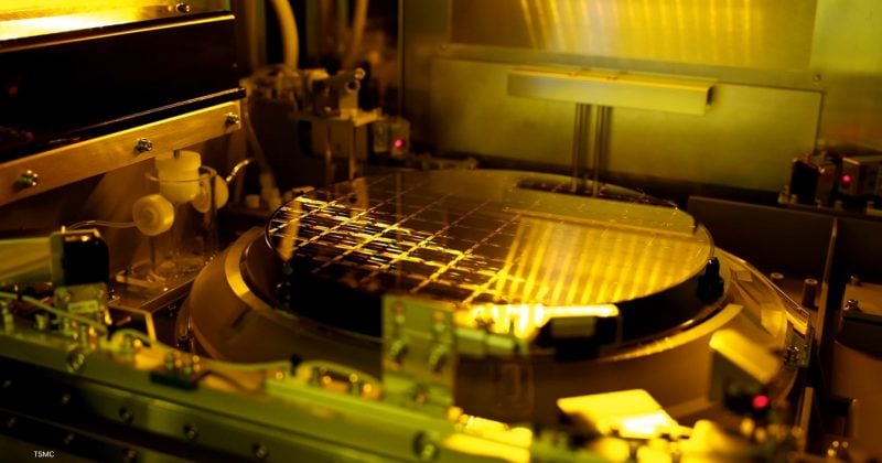
NVIDIA said TSMC is using its accelerated computing and AI technologies to advance semiconductor design and manufacturing, bringing AI systems deeper into the world’s most important chip production lines.
The companies said TSMC is applying NVIDIA tools across the semiconductor lifecycle to improve turnaround time, energy efficiency, yield, and operational productivity in advanced fabs. The work spans computational lithography, transistor simulation, process control, wafer inspection, and fab operations.
As chips move to more advanced nodes, bringing designs into high volume production has become one of the semiconductor industry’s most complex computing problems. NVIDIA said these processes now require massive scale simulation, real time optimization, and AI systems that can support physics, imaging, and manufacturing workflows.
Jensen Huang, founder and CEO of NVIDIA, said TSMC is bringing NVIDIA AI and accelerated computing into the fab itself to tackle complex design and manufacturing challenges with simulation, optimization, and AI.
TSMC is using NVIDIA CUDA X libraries and AI models on NVIDIA GPUs to accelerate several core manufacturing workloads. The company is using cuLitho for computational lithography, with NVIDIA saying the GPU accelerated library can deliver a 20% to 50% improvement in cost effectiveness or cycle time compared with CPU based lithography while maintaining the same cost of ownership.
TSMC is also using NVIDIA cuEST, a GPU accelerated electronic structure simulation library, for semiconductor material design. NVIDIA said cuEST can deliver 50 times faster chemistry simulations on average.
For process control, TSMC is using NVIDIA cuML to accelerate large scale analytics on NVIDIA GPUs, helping distill hundreds of thousands of process parameters across thousands of steps into more precise machine learning inputs. NVIDIA said the work is aimed at reducing process variation across advanced manufacturing.
TSMC is also using NVIDIA H200 GPUs and CUDA powered scheduling computation to improve fab operations and manage complex production constraints. The companies said the approach helps streamline production paths and improve fab productivity.
The collaboration also extends into defect inspection. TSMC is using NVIDIA Metropolis and the NVIDIA TAO Toolkit to improve advanced defect classification with vision AI, helping detect defects at nanometer scale while reducing the need for repeated labeling and retraining as process conditions change.
TSMC is also exploring NVIDIA Omniverse libraries to build FabTwin, a virtual fab environment for evaluating process tool layouts and simulation workflows. The system is designed to let TSMC test fab design scenarios digitally before physical implementation, helping identify potential constraints earlier and improve planning efficiency.
The announcement deepens a nearly three decade partnership between NVIDIA and TSMC. It also shows NVIDIA moving further into the semiconductor manufacturing stack at a time when demand for AI chips is increasing pressure on advanced fabs, chip design workflows, and global manufacturing capacity.