Tata Electronics partners with ASML to build India’s first semiconductor fab
The Dholera facility will focus on mature-node chips, backed by massive government subsidies and collaboration with Taiwan's PSMC.
Tata Electronics and ASML, the Dutch company that holds a near-monopoly on the lithography machines essential to chipmaking, have announced a strategic partnership to support India’s first semiconductor fabrication plant. The facility, located in Dholera, Gujarat, represents the most concrete step yet in India’s long-running ambition to stop importing virtually all of its chips.
What’s actually being built
The Dholera fab will be a 300mm facility, which is the industry standard wafer size for modern chip production. It’s designed to produce 50,000 wafers per month, targeting analog and logic chips using process technologies ranging from 28nm to 110nm.
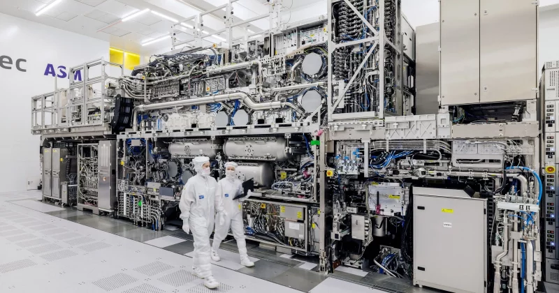
The technology for the fab is being developed in collaboration with Taiwan’s Powerchip Semiconductor Manufacturing Corp (PSMC). ASML’s role is arguably even more critical. Every modern chip fab on the planet needs ASML’s lithography systems, the machines that use light to etch circuit patterns onto silicon wafers.
The money behind it
The total investment is projected at ₹91,000 crore. The central government is covering 50% of the project cost, with the Gujarat state government contributing an additional 20%. That means roughly 70% of the funding is coming from public coffers, leaving Tata to cover the remaining share.
Why ASML matters here
ASML is not just another equipment vendor. The company, headquartered in Veldhoven, Netherlands, is the sole manufacturer of extreme ultraviolet (EUV) lithography machines and the dominant supplier of the deep ultraviolet (DUV) systems that fabs operating at 28nm and above rely on.
For Tata’s Dholera fab, the relevant technology is DUV lithography, since the facility’s 28nm-to-110nm range doesn’t require EUV. But even DUV machines are extraordinarily complex, costing tens of millions of dollars each, and ASML’s involvement signals that the Dholera project is being built to genuine industry standards rather than as a symbolic gesture.