US invests $250M in I-Pulse for semiconductor and pulsed-power development under CHIPS Act
The Department of Commerce is funding a company that repurposed military pulsed-power technology for civilian semiconductor manufacturing
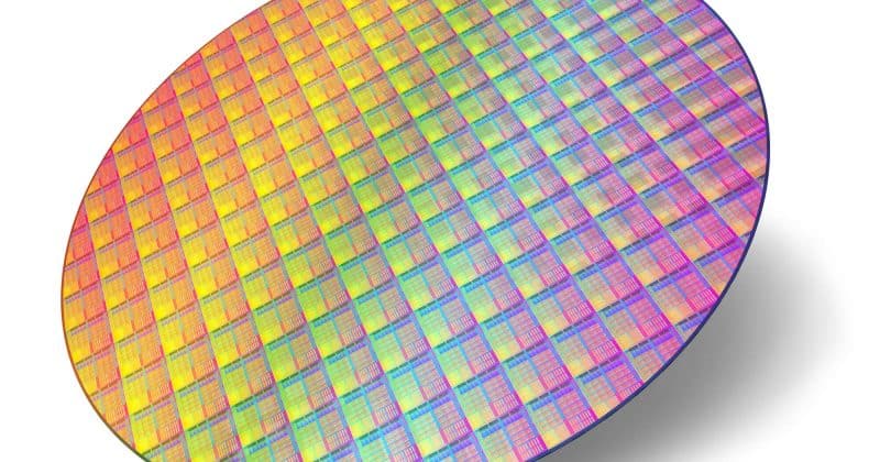
The US Department of Commerce has signed a definitive agreement to invest $250 million in I-Pulse, a privately held company that specializes in high pulsed-power systems. The funding comes through the CHIPS and Science Act and is specifically targeted at research and development for high-temperature, high-performance semiconductors.
From weapons labs to wafer fabs
I-Pulse was co-founded in 2007 by Robert Friedland and Laurent Frescaline. The company is based in Albuquerque, New Mexico, which is fitting given that its pulsed-power technology traces its origins to research conducted at Sandia National Laboratories, one of the US government’s premier defense research facilities.
Until now, I-Pulse has primarily applied this technology to mining, geothermal drilling, and mineral exploration. The CHIPS Act funding essentially bankrolls the company’s expansion into semiconductor development, where those same precise energy discharges could prove useful in manufacturing next-generation chips that operate at higher temperatures and performance levels than current designs.
The company had already raised over $324 million in previous funding rounds, including investments from Ivanhoe Mines. So this $250 million federal infusion nearly doubles its total capital base.
The company has also been expanding its civilian footprint beyond semiconductors. In March 2026, I-Pulse announced a strategic partnership for geothermal drilling projects in Australia, collaborating with Sunrise Energy Metals and Greenvale Mining.
What this means for investors and the broader market
The $250 million investment fits squarely within Washington’s broader strategy to reshore semiconductor manufacturing. The CHIPS and Science Act has already funneled billions into companies like Intel, TSMC, and Samsung for building fabrication plants on US soil. Rather than subsidizing a known quantity to build a factory, the government is placing a bet on a relatively niche technology company with roots in defense research.
Established players in the silicon carbide space, like Wolfspeed and STMicroelectronics, have been investing heavily in capacity. I-Pulse entering this arena with a fundamentally different manufacturing approach, backed by substantial federal dollars, could reshape how the market thinks about production methods for advanced semiconductor materials.
I-Pulse is transitioning from mining and energy applications into semiconductor manufacturing, which is one of the most technically demanding industries on the planet. The gap between laboratory breakthroughs and commercial-scale manufacturing has buried plenty of promising companies before.