SK Hynix plans to triple wafer capacity by 2034 to meet AI demand
South Korea's memory chip giant is betting tens of billions on the AI boom with four new fabs and a roadmap to triple production in under a decade
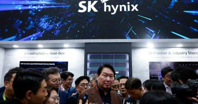
SK Hynix, the company that makes the memory chips powering virtually every cutting-edge AI system on the planet, just laid out one of the most aggressive expansion plans the semiconductor industry has ever seen. The goal: triple its wafer production capacity by 2034.
SK Group Chairman Chey Tae-won disclosed the timeline in a Nikkei Asia interview, outlining a phased approach that starts with doubling capacity by around 2031 before reaching the triple mark three years later. Four new fabrication facilities at the Yongin Semiconductor Cluster in South Korea will anchor the effort, with the first cleanroom targeted for early 2027.
The numbers behind the buildout
The scale here is staggering. Phase 1 alone carries an investment tag of over KRW 21.6 trillion. And that’s just one piece of the puzzle.
In April 2026, SK Hynix separately committed roughly $13 billion to a new advanced packaging plant. That facility is designed specifically to meet demand for high-bandwidth memory, the specialized DRAM that sits atop AI processors from companies like NVIDIA and allows them to crunch data at speeds that standard memory simply can’t match.
The company’s near-term target is to nearly double DRAM wafer production to approximately one million wafers per month by 2030-2031.
SK Hynix has sold out its entire HBM production through 2026. Every chip it can make already has a buyer.
Why HBM is the new oil
HBM is stacked vertically and bonded directly to the GPU using advanced packaging techniques, restructuring memory to feed data to AI processors as fast as they can consume it.
SK Hynix currently commands somewhere between 50% and 70% of the global HBM market. That kind of dominance in a component this critical to AI infrastructure gives the company enormous pricing power and strategic leverage.
Market reaction and competitive landscape
Investors have noticed. SK Hynix shares rebounded in June 2026 on the capacity expansion news, with the company’s market valuation reaching or approaching $1 trillion.
Samsung, SK Hynix’s chief rival in memory, has been scrambling to catch up in HBM after quality issues delayed its entry into NVIDIA’s supply chain. Micron, the American competitor, has also been investing heavily but operates at a smaller scale in this specific product category.
The risk to watch is execution. Building four fabs simultaneously while ramping an advanced packaging plant is an operational challenge that even the best-run semiconductor companies can stumble on. Yield rates on cutting-edge HBM stacking remain technically demanding, and any delays at the Yongin cluster could leave the company unable to meet its own aggressive targets.