Tensordyne claims 13x throughput improvement over Nvidia’s NVL72 GB300 with new TDN AI Processor
A Sunnyvale startup says its logarithmic math chip can process 363,000 tokens per second per rack, dwarfing Nvidia's current inference hardware
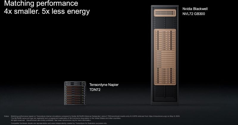
Tensordyne, a startup with offices in Sunnyvale and Munich, announced its Napier (TDN) AI inference processor on June 15, claiming its TDN72 rack-scale system delivers 13 times higher throughput in tokens per second and 17 times more tokens per watt than Nvidia’s GB300 NVL72 rack. The comparison benchmark: DeepSeek-R1 inference workloads.
The numbers behind the claim
Tensordyne says a single rack running its hardware can churn out roughly 363,000 tokens per second. The company pegs Nvidia’s equivalent rack at approximately 27,400 tokens per second on the same workload.
The secret sauce is something called a logarithmic number system, or LNS, executed directly in hardware. Instead of doing math the way conventional chips do (multiplying big floating-point numbers together), LNS converts multiplication into addition, which is dramatically cheaper in terms of transistors and energy. It’s a technique that’s been studied in academia for decades but has historically been too impractical for production silicon.
Tensordyne built its Napier chip on TSMC’s 3nm process node, integrating both SRAM and HBM memory on-package. The full rack configuration stacks four pods of 72 chips each, totaling 288 chips, with a target power envelope of roughly 120 kW for the entire rack. That’s air-cooled, not liquid-cooled.
The company developed its high-speed scale-up interconnect in collaboration with Broadcom and HPE Juniper. Broadcom contributes silicon development expertise, and HPE Juniper provides data center interconnect capability.
Production timeline and demand signals
Tensordyne says it has accumulated over $200 million in letters of intent and evaluations. Volume production is targeted for mid-2027, with initial shipments expected in late 2026.
The company’s pitch to customers is that each rack could generate tens of millions of dollars more in annual revenue compared to an equivalent Nvidia deployment.
Why this matters for the AI hardware market
Inference workloads are more predictable than training and can be optimized for specific model architectures. By focusing exclusively on inference rather than competing across the full training-and-inference stack, Tensordyne sidesteps Nvidia’s strongest competitive advantages.
The 3nm TSMC process choice puts Tensordyne on roughly the same manufacturing node as Nvidia’s upcoming chips, meaning the performance gap, if real, comes from architectural innovation rather than a process node advantage.
Investors should watch for third-party benchmark validation, which should arrive around the time of initial shipments in late 2026.