Intel’s EMIB-T takes aim at TSMC’s CoWoS-L as AI chip packaging gets crowded
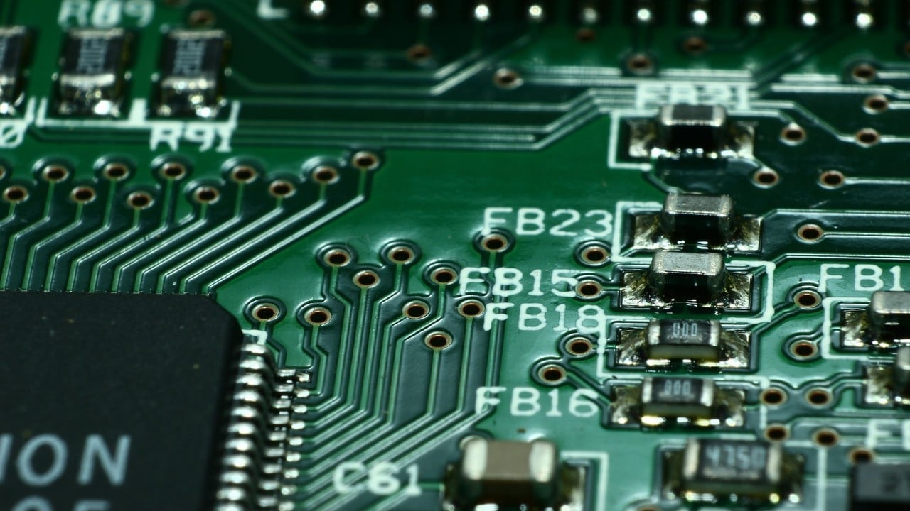
Photo: Pixabay / Pexels
Intel is pitching its bridge-based packaging as a higher-yield, lower-cost alternative while TSMC's CoWoS capacity stays fully booked
Intel wants a bigger piece of the AI chip boom, and it is not starting with the chips themselves. It is starting with the packaging that holds them together.
The company expects future AI packages to carry more than 32 HBM stacks and over 70 EMIB bridges. That is a lot of hardware crammed into one slab, and Intel is betting its EMIB-T technology can handle it more efficiently than TSMC’s CoWoS-L.
What Intel is actually selling
TSMC’s CoWoS approach has historically leaned on a large silicon interposer, essentially a big slab of silicon that everything sits on. CoWoS-L, the version in question, is the variant now drawing direct comparisons with Intel’s offering.
Intel’s EMIB-T takes a different route. Instead of one giant silicon foundation, it embeds small, localized silicon bridges inside an organic substrate, placing silicon only where chips need to talk to each other.
The “T” adds through-silicon vias (TSVs), which are vertical electrical connections running through the bridge. Put simply, they give power a more direct path into the package, which matters when chips are this hungry.
Intel’s Foundry Packaging Director, Kyu-oh Lee, made the efficiency case at the ISMP 2026 event in Busan on November 4, 2026. According to Lee, EMIB achieves wafer utilization above 90%, compared with roughly 60% for conventional interposer designs.
That gap matters more than it sounds. Wafer utilization measures how much of each silicon wafer ends up as usable product. When you only need small bridges instead of a huge interposer, far less expensive silicon goes to waste.
The scaling roadmap
Intel’s targets get progressively more ambitious. For the 2026-2027 window, the company is aiming at designs larger than 120 × 180 mm, carrying 16 or more HBM stacks and at least 38 EMIB bridges.
AI, tech, and the markets they move—in one daily briefing.
Daily. Free. Join 34,000+ readers across crypto, finance, and policy.
After that, Intel projects AI packages reaching 240 × 240 mm, with more than 32 HBM stacks and over 70 EMIB bridges.
EMIB-T is slated to enter production in 2026. Intel says it will support packages extending beyond 8-9x reticle size.
On yields, EMIB-T is reportedly approaching 90%. The weak spot is the substrate, the organic base the bridges sit in, where yield remains a noted issue.
TSMC’s CoWoS yields are reportedly near 98%. That is the bar Intel has to clear, and an eight-point gap is not nothing when each package holds some of the most expensive silicon on the planet.
Why this fight is happening now
The simplest explanation is supply. CoWoS capacity, particularly CoWoS-L, is fully booked. When the dominant supplier has no room, customers start shopping around.
That has sharpened interest in EMIB-T as a lower-cost option. Google, Amazon, and MediaTek have been named as potential adopters, with Google and Amazon described as exploring the technology for future AI chip designs.
TSMC is hardly standing still. The company is scaling CoWoS-L and also looking into bridge-based designs of its own. It plans to keep CoWoS-L as its mainstream solution through 2028.
What this means for the AI hardware race
For Intel, packaging may be the most realistic foothold in a market where TSMC has dominated leading-edge manufacturing. Customers do not necessarily need Intel to fabricate their chips to use Intel’s packaging, which lowers the barrier to giving it a try.
The wafer utilization argument is Intel’s strongest card. If more of every wafer becomes sellable product, the cost per package should fall, and buyers facing tight supply care about both price and availability.
The risk sits in the yield numbers. A package carrying dozens of HBM stacks concentrates enormous value in one unit. A substrate defect that scraps the whole assembly gets costly fast, which is why the reported gap between roughly 90% and near 98% deserves attention.
What to watch: whether EMIB-T hits its 2026 production timeline, whether substrate yields close the distance with TSMC, and whether Google, Amazon, or MediaTek move from evaluation to committed volume. Equally telling will be how far TSMC pushes its own bridge-based work before 2028.
Disclosure: This article was edited by Diego Almada Lopez. For more information on how we create and review content, see our Editorial Policy.